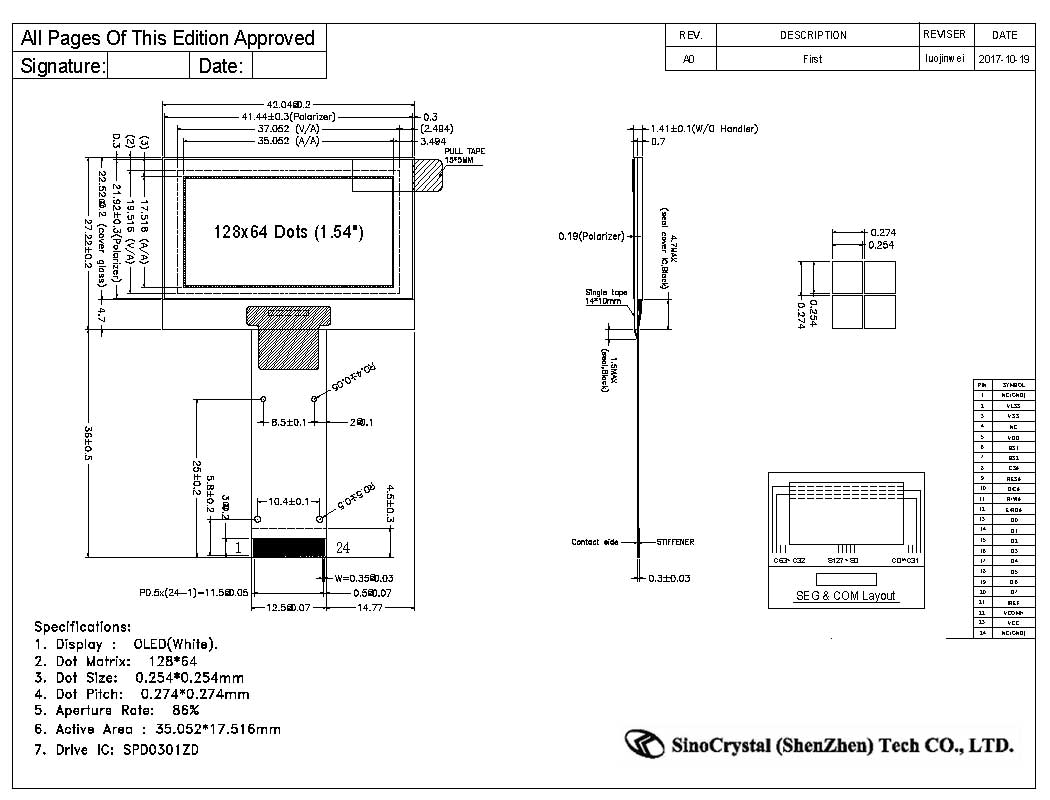
General Specification
| ITEM | SPECIFICATIONS | UNIT |
| MODULE SIZE | 42.04(W)x27.22(H)x1.41(D) | mm |
| VIEWING AREA | 37.052 (W) x 19.516(H) | mm |
| ACTIVE AREA | 35.052(W) x17.516(H) | mm |
| DOT SIZE | 0.254(W) x0.254(H) | mm |
| DOT PITCH | 0.274(W) x0.274 (H) | mm |
| ASSY.TYPE | COG | — |
| WEIGHT | TBD |
Interface Definition
| PIN NO. | SYMBOL | TYPE | FUNCTION DESCRIPTIONS |
| 1 | NC(GND) | P | It should be connected to external ground. |
| 2 | VLSS | P | This is an analog ground pin. It should be connected to VSS externally. |
| 3 | VSS | P | Ground pin. It must be connected to external ground. |
| 4 | NC | NC | |
| 5 | VDD | P | Power pin for logic circuit. It must be connected to external source. |
| 6 | BS1 | I | Interface selection pins. I2C680080804SPIBS11010BS20110 |
| 7 | BS2 | ||
| 8 | CS# | I | Chip Select input pin. Active “L” |
| 9 | RES# | I | Hardware reset input pin. Active “L”. |
| 10 | D/C# | I | WThis is Data/Command control pin. When the pin is pulled HIGH, the data at D[7:0] is data. When the pin is pulled LOW, the data at D[7:0] is command. In I2C mode, this pin acts as SA0 for slave address section. When 3-wire serial interface is selected, this pin must be connected to VSS |
| 11 | R/W# | I | This is read/write control input pin. 8080: data write enable; 6800: read/write select pin. When serial or I2C interface is selected, this pin must be connected to VSS. |
| 12 | E/RD# | I | This is read/write control input pin. 8080: data read enable; 6800: read/write enable pin. When serial or I2C interface is selected, this pin must be connected to VSS. |
| 13 | D0 | I/O | These are 8-bit bi-directional data bus to be connected to microprocessor’s Data bus. When serial interface mode is selected, D2 should be kept NC, D1 will be the serial data input: SDIN, D0 will be the serial clock input: SCLK. When I2C mode is selected, D2, D1 should be tied together and serve as SDA and D0 is the serial clock input, SCL. |
| 14 | D1 | ||
| 15 | D2 | ||
| 16 | D3 | ||
| 17 | D4 | ||
| 18 | D5 | ||
| 19 | D6 | ||
| 20 | D7 | ||
| 21 | IREF | I | Current reference for brightness adjustment. This is segment output current reference pin. A resistor should be connected between this pin and VSS .Set the current at 10 uA maximum. |
| 22 | VCOMH | O | COM signal deselected voltage level. A capacitor should be connected between this pin and VSS. |
| 23 | VCC | P | Power supply for OLED driving voltage. A capacitor should be connected between this pin and VSS. |
| 24 | NC(GND) | P | It should be connected to external ground. |
Previous Product Previous Product : 1.41'' MIPI OLED With 320*360 Dot Matrix ZTW522 IC
Next Product : 2.7'' 128×64 SSD1325 OLED Graphic Display Next page