The article mainly introduces the TFT LCD open cell process. The TFT LCD open cell process is generally divided into front, middle and back processes. The front process is mainly for the production of TFT glass; the middle process mainly refers to the pasting of TFT glass and color filters. Bonding; The back-end manufacturing process refers to the pressing of the driver IC, printed circuit board and liquid crystal panel. The author believes that only by understanding the entire TFT LCD open cell process can the TV backlight system, motherboard and even the entire TV design be better.
1. Brief description of TFT LCD open cell manufacturing process
The TFT LCD open cell process is generally divided into front, middle and back processes. The front process is mainly for the production of TFT glass, which is very similar to the semiconductor process; the middle process mainly refers to the bonding of TFT glass and color filters, and Add the upper and lower polarizing plates; the latter process refers to pressing the driver IC and the printed circuit board to the TFT glass, and completing the open cell as we know it.
2. Front-end process of TFT LCD open cell
7 The front-end process of TFT LCD open cell is very similar to the semiconductor process, mainly divided into four steps:
1. Use precipitation to form gate metal. First, coat a layer of metal on the glass substrate, then coat the photoresist, and finally form gate metal through exposure, development, etching and degumming. The main components of the coated metal materials are: titanium (TI), aluminum (AL), molybdenum (MO) and chromium (CR) and their mixtures.
2. Precipitating SI3N4 (silicon nitride), a-SI (amorphous silicon) and N+a-si (N-type silicon). First, use PECVD (Plasma Enhanced Chemical Vapor Deposition) technology to coat a layer of SI3N4, N+a-si and a-si respectively, and then coat photoresist on N+a-si and a-si, through exposure and development , Etch and remove glue to form the desired shape. PECVD refers to plasma-enhanced chemical vapor deposition. The principle is to use microwave or radio frequency to ionize the gas containing the atoms of the film to form a plasma locally. The plasma has a strong chemical activity and is easy to react on the substrate. The desired film is deposited. The roles played by the three materials of SI3N4, N+a-si and a-si are: gate terminal and electrolyte of liquid crystal storage capacitor, N-type semiconductor and P-type semiconductor.


3. Form source metal and drain metal. First, a layer of metal material is coated on the a-si as the source metal and drain metal, and then the photoresist is coated on the metal material and the desired shape is formed by exposure, development, etching and degumming. The main components of source metal and drain metal are titanium (TI), aluminum (AL), molybdenum (MO) and chromium (CR), which are the same as gate metal.
4. Precipitating SI3N4 and ITO (Indium Tin Oxides), ITO indium tin oxide is a transparent conductive film. First, a layer of SI3N4 is deposited by PECVD technology, and then a layer of ITO is coated. At this point, the entire TFT glass is completed. That is to say, the front-end process of TFT LCD open cell has been completed. Its architecture is shown in Figure 4, where the gate metal is connected to Gate ic, source metal is connected to data ic.


3. TFT LCD open cell mid-stage process
The 7 inch display structure is like a sandwich, with liquid crystal sandwiched between the lower TFT glass and the upper color filter. The mid-stage process of TFT LCD open cell is also divided into four main steps:
1. Pre-treatment of lower TFT glass pressing. First, use ionized water to clean the front TFT glass, and then coat a layer of organic polymer alignment film on the surface of the TFT glass, and then form the so-called PI alignment film by rolling. Its main function is to make a special film for liquid crystal molecules. There is a channel with a fixed angle to control its rotation direction and angle under the action of voltage. Then apply a rectangular sealant on the TFT glass to facilitate the adhesion of the TFT glass and the color filter and prevent the leakage of the liquid crystal, and this rectangle will be the visible area of the open cell, and finally inject it into the plastic frame liquid crystal.

2. The upper color filter is processed before pressing. First, an organic polymer material is coated on the color filter substrate, and then an alignment film is formed by rolling. Then spray spacers in the color filter to ensure the gap between the color filter and the TFT substrate.

3. Press the TFT glass substrate and the color filter, and apply conductive glue on the frame part of the press to ensure that external electrons can enter the liquid crystal layer. The order from top to bottom after pressing is: color filter, alignment film, liquid crystal, alignment film and TFT glass.

4. Cut the laminated liquid crystal panel according to the set size, and then paste the horizontal polarizing plate and the vertical polarizing plate on the cut liquid crystal panel. So far, the mid-stage process of the entire TFT LCD OPEN CELL has been completed.
Fourth, TFT LCD open cell back-end manufacturing process
The back-end process of TFT LCD open cell mainly refers to pressing the driver IC and PCB onto the LCD panel. This process mainly consists of three steps:
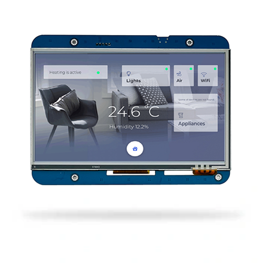
Touch screen 7 inch is designed for embedded and portable equipment projects, and has the best compatibility with LattePanda alpha & delta, without any configuration and additional cables, plug and play
1. Coating of ACF (Anisotropic Conductive Film). Apply ACF where the LCD panel needs to press the driver IC. ACF is also called anisotropic conductive adhesive film. It is characterized by conduction in the up and down direction and non-conductive in the left and right directions. Its main function is to connect the driver IC and the LCD panel.

2. The pressing of the driver IC. The driver IC is pressed onto the ACF-coated liquid crystal panel, which is often referred to as bonding in the liquid crystal manufacturing process. The driver IC is generally COF (Chip On FPC) material, and is divided into gate IC and date IC. The gate IC is connected to the GATE terminal of the TFT glass mentioned above to control the switching of TFT; the date IC is connected to the source terminal of the TFT glass. Charge the liquid crystal capacitor to control the voltage across the liquid crystal.

3. PCB pressing. Press the PCB to the date IC end of the LCD panel, then the IC on the PCB can directly control the date IC and can transmit the signal to the gate IC through the date IC to control the gate IC. So far, the entire TFT LCD open cell manufacturing process has been completed, and an open cell as we know it has been produced.

Sinocrystal HOT LCD has launched a series of high brightness TFT LCD solutions for customers to choose from. The brightness of the high-brightness TFT display is as high as 800 ~ 1000 nits. At present, the sizes of visible TFT modules available under the sun are 2.4 inch TFT, 2.8 inch, 3.5 inch, 4.3 inch, 5.0 inch, 7 inch, 10.1 inch, etc. The high-brightness TFT liquid crystal display is suitable for outdoor terminals (industrial equipment such as measuring equipment, prospecting equipment, testing equipment, etc.) that require sunlight.

The 8 inch displays might be affected and delay for an accident.
LCM, namely LCD display module and LCD module, refers to the assembly of LCD devices, connectors, peripheral circuits such as control and drive, PCB circuit board, backlight, structural parts, etc. In the home theater, LCD has become the mainstream, bringing joy to more families.
New iPhone 13 Series will use On-Cell OLED Displays. And it that will be launched in the second half of this year will be exclusively supplied by Samsung Display (SDC)
Top 10 LCD Display Manufacturers in China (2026 Guide for OEM Buyers)
Sinocrystal provides a secure and reliable packaging system for LCD displays, ensuring maximum protection against shock, moisture, and static electricity during global transportation.
Discover how LCD displays are evolving in industrial automation — from high-brightness and rugged designs to smart connectivity and energy efficiency. Explore what’s next for industrial-grade visual interfaces.
Discover the key factors to consider when choosing an LCD display for your project, including size, resolution, interface, brightness, and customization options from a factory-direct manufacturer.